In context: As we approach the 2nm process node, some roadblocks are emerging that could further stagnate the already slow Moore's Law progress. One challenge is how to efficiently distribute power to tens of billions of tiny transistors using copper wiring without eroding performance gains. Now, Applied Materials, a major supplier of semiconductor manufacturing equipment, believes it has the answer.
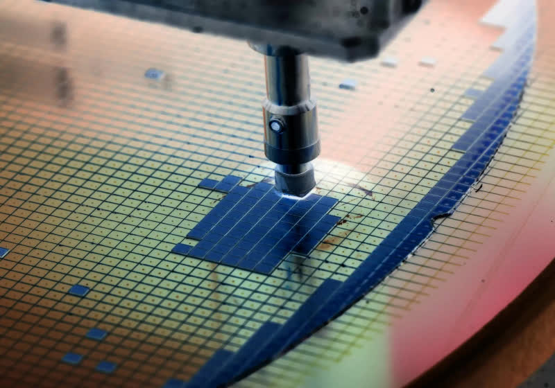
Last week, Applied Materials pulled back the curtain on its latest materials engineering solutions designed to enable copper wiring to scale down to 2nm dimensions and below while also reducing electrical resistance and strengthening chips for 3D stacking. The company's Black Diamond low-k dielectric material has been offered since the early 2000s. It surrounds copper wires with a special film engineered to reduce the buildup of electrical charges that increase power consumption and cause interference between electrical signals.

Applied Materials has now come up with an enhanced version of Black Diamond, which reduces the minimum k-value even further, enabling copper wiring scaling to the 2nm node while also increasing mechanical strength – a critical property as chipmakers look to stack multiple logic and memory dies vertically. But scaling the copper wiring itself as dimensions shrink is another enormous challenge. Today's most cutting-edge logic chips can pack over 60 miles of copper wires that are fashioned by first etching trenches into the dielectric material and then dep.